Lab-Grown Diamond Wafers for Next-Generation Electronics
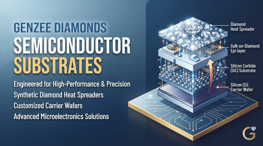
At Genzee Diamonds, our Chemical Vapor Deposition (CVD) expertise extends beyond gem-quality jewelry stones into one of the most demanding materials markets in the world: semiconductor-grade diamond substrates. Using the same precision growth and laser micro-machining capabilities that define our jewelry production, we manufacture single-crystal and polycrystalline diamond wafers engineered for power electronics, RF/microwave components, and advanced thermal management applications.
Diamond is widely regarded as the ultimate wide-bandgap semiconductor material. It combines the highest thermal conductivity of any known solid with an exceptionally wide bandgap and high breakdown voltage — properties that let electronic devices run hotter, faster, and more efficiently than substrates built on silicon, silicon carbide, or gallium nitride alone.
Why Diamond Outperforms Conventional Substrates
| Property | Typical Silicon | Diamond (CVD) |
|---|---|---|
| Thermal Conductivity | ~150 W/m·K | Up to ~2,000+ W/m·K |
| Bandgap | ~1.1 eV | ~5.5 eV |
| Breakdown Field | Low | Very High |
| Operating Temperature Limits | Limited | Extends well beyond conventional wide-bandgap materials |
| Chemical/Radiation Resistance | Moderate | Excellent |
Because diamond conducts heat away from a chip’s hotspot far more effectively than copper or silicon, devices built on or bonded to diamond substrates can sustain higher power densities without throttling — a critical advantage as chips in AI computing, EV power modules, and RF systems continue to shrink while power demands rise.
Our Substrate Offerings
Single-Crystal Diamond (SCD)
Grown as a monolithic crystal for applications that demand the lowest defect density and highest optical/electronic purity — ideal for epitaxial growth platforms, high-voltage diamond devices, and quantum-grade substrates.
Polycrystalline Diamond (PCD)
Larger-format wafers produced at scale for high-volume thermal management applications, including heat spreaders bonded beneath power dies and RF modules.
Substrates are available in a range of standard plate sizes and wafer diameters, with custom dimensions, thicknesses, crystal orientations, surface polishing, and doping levels (including boron-doped, conductive-grade diamond) available on request.
Applications
- Power Electronics — High-voltage diodes, transistors, and inverters operating at elevated junction temperatures beyond the practical limits of silicon or silicon carbide.
- RF & Microwave Devices — Low-loss diamond substrates supporting high-power, high-frequency transistor and amplifier designs, including diamond-on-substrate configurations for next-generation wireless infrastructure.
- Thermal Management — Diamond heat spreaders and submounts placed beneath high-power dies to pull heat away laterally, protecting performance and extending hardware lifespan.
- Quantum Technology — Ultra-pure, low-nitrogen diamond material suited to nitrogen-vacancy (NV) center research and quantum sensing platforms.
- Aerospace & Defense — Radiation-hard, high-temperature-tolerant substrates for demanding field and space environments.
- Optoelectronics — Diamond’s broad optical transparency and chemical inertness support detector and photonic device development.
Full Characterization, Every Wafer
Every semiconductor substrate we produce ships with documentation your engineering and quality teams can rely on, including:
- Surface roughness and thickness mapping
- Crystal quality and stress verification
- Nitrogen content classification
- Dimensional reporting (bow, warp, and thickness uniformity)
Why Manufacture With Genzee Diamonds
Genzee Diamonds is a U.S.-based (Sugar Land, Texas) lab-grown diamond manufacturer with an international team of materials researchers and process engineers. Our CVD reactors, nanometer-scale manufacturing methods, and laser micro-precision finishing — originally developed for flawless gem-quality diamond production — translate directly into the tight tolerances and material purity that semiconductor and electronics customers require. We support custom specifications, OEM/ODM partnerships, and flexible order volumes, from prototype samples to production-scale supply.
Request a Quote
Whether you’re prototyping a new power device, sourcing thermal substrates for a production run, or evaluating diamond for a quantum sensing application, our team can work with you on custom specifications and sample orders.
Contact us: 786@genzeediamonds.com